1) Which resistance is offered by the diode in forward direction above the barrier voltage?
a. Bulk Resistance
b. Junction Resistance
c. Dynamic Resistance
d. Reverse DC Resistance
|
Answer
Explanation
|
ANSWER: Bulk Resistance
Explanation:
Bulk resistance is the sum of resistance values of P & N type semiconductor materials. Because of its minute value, bulk resistance can also be expressed as,
rB = ( VF - VB ) / IF
When the value of current is very large, the diode offers the resistance above the barrier voltage in forward direction.
On the contrary, junction resistance solely depends on the magnitude of forward DC current & hence ultimately known as 'Variable Resistance'. Dynamic resistance is almost equal to junction resistance for negligible values of rB and IF. Apart from these, reverse DC resistance is offered in case of reverse voltage corresponding to reverse current absolutely in reverse direction.
|
|
2) Which basic Op-amp regulator allows to increase the emitter voltage until the value of inverting input voltage becomes equal to Zener voltage especially when increased voltage is applied to the base of transistor?
a. Op-amp Series Regulators
b. Op-amp Shunt Regulator
c. Both a & b
d. None of the above
|
Answer
Explanation
|
ANSWER: Op-amp Series Regulators
Explanation:
As per the configurational arrangement, due to decrease in input voltage or load current, output voltage also tend to decrease. Thus, it is essential to apply the proportional voltage decrease to an inverting output of Op-amp using potentiometer. As another op-amp input is under the hold of Zener voltage at a fixed reference value, it gives rise to a small difference voltage across the two inputs of op-amp.
This difference voltage is also known as error voltage and it is amplified due to which the output voltage increases. Increased output voltage is further applied to the base of transistor by rising the value of emitter voltage till the inverting input voltage becomes equal to reference or Zener voltage.
This action eventually offsets attempted decrease in output voltage by maintaining it at certain value.
|
|
3) Compute the values of VOUT & P1 in a variable feedback regulator circuit with Vin = 20V, Vz = 12V & RL = 2K if the transistor is of silicon and the wiper of R3 is adjusted in half-way configuration.
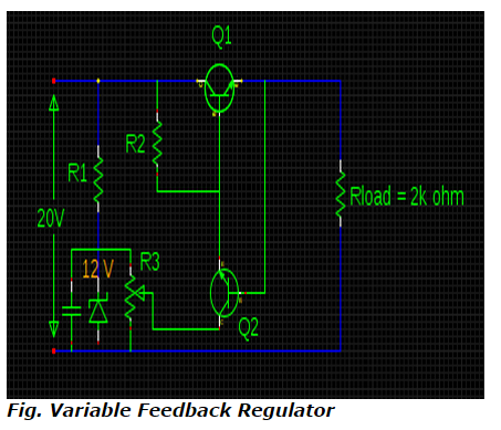 a.
a. 16.8 V & 137.76 mW
b. 10.7 V & 80.09 mW
c. 6.7 V & 43.89 mW
d. 4.7 V & 35.79 mW
|
Answer
Explanation
|
ANSWER: 6.7 V & 43.89 mW
Explanation:
From the configuration of feedback regulator circuit,
VOUT = Voltage at wiper + VBE2
Voltage at wiper must be equal to half the Zener voltage since wiper is adjusted in half way configuration.
VOUT = (12 / 2) + 0.7
= 6.7 V
P1 = VCE1 x IE1
But, VCE1 = Vin - Vout
= 20 – 6.7
= 13.3 V
IE1 = IL = Vout / RL = 6.7 /2k = 3.3 mA
Therefore, P1 = 13.3 x 3.3 = 43.89 mW
|
|
4) Which transistor regulator is also known as 'Emitter-Follower Regulator'?
a. Transistor Series Voltage Regulator
b. Controlled Transistor Series Regulator
c. Transistor Shunt Voltage Regulator
d. Transistor Current Regulator
|
Answer
Explanation
|
ANSWER: Transistor Series Voltage Regulator
Explanation:
The circuit configuration of transistor series voltage regulator is in such a manner that voltage at the emitter follows the base voltage.
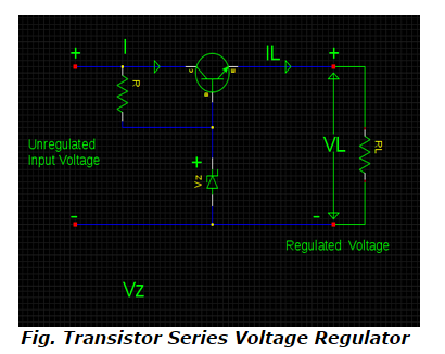
Even the transistor in this type of set-up acts as a variable resistor whose value of resistance is determined by the base current. This transistor is also known as pass transistor because it allows to pass the current that needs to be regulated through it.
|
|
5) Which equation represents the output voltage of fixed negative linear voltage regulator?
a. V OUT = V fixed + [(V fixed / R 1) + I Q] R 2
b. V OUT = - {V fixed + [(V fixed / R 1) + I Q] R 2}
c. V OUT = V fixed [( R 1 + R 2) / R 2]
d. V OUT = - {V fixed [(R 1 + R 2) / R 2]}
|
Answer
Explanation
|
ANSWER: VOUT = Vfixed [( R1 + R2) / R2]
Explanation:
Fixed Negative Voltage Regulator offers a fixed level of negative voltage. Usually, 7900 series regulator with three terminal IC configuration is widely used . The capacitor (typical value of 0.22 μF) is necessary only when the location of power supply is 3 inches far from the IC regulator circuit.
Also, capacitor C2 is essential to obtain the stability of output voltage whose value is supposed to be 1μF
It is mandatory to connect the capacitor (C3) in order to ameliorate the transient response of the output voltage.
The output voltage can be generally represented by,
VOUT = Vfixed [(R1 + R2 ) / R2]
Usually, the output voltage obtained from fixed voltage negative regulator lies in the range of -5V to -12 V.
On the contrary, the output voltage of fixed positive linear voltage regulator can be adjusted within the range of 5V to 15 V and can be expressed as,
VOUT = Vfixed + [(Vfixed / R1) + IQ] R2
(Remaining equations are just meant to create perplexity)
|
|
6) Commercial IC Voltage Regulators have greater significance because of their unique in-built characteristic/s like ____
a. Fold-back Current-limiting
b. Remote Control Operation
c. Self-protection against temperature
d. All of the above
|
Answer
Explanation
|
ANSWER: All of the above
Explanation:
IC Voltage Regulators are simple in configuration and provide fixed voltage with better quality of precision level. These IC regulators performs with greater improved features as compared to the conventional ones made from discrete components.
Some of the salient features of IC regulators include current limiting strategy, self-protection against excessive temperature along with the remote control operation for a maximum range of input voltages. Besides these, it comprises an additional feature of foldback current limiting with proficiency at functioning level.
These IC Voltage regulators are categorized into fixed & adjustable positive and negative linear voltage regulators depending on the performance & mode of operation.
|
|
7) Which filter provides the smoothing effect over the repetitive charging & discharging phases of capacitor generated by repetitive ON-OFF action of the transistor in an inverting type of switching regulator?
a. LC filter
b. RC filter
c. R-L-C filter
d. C-L-C filter
|
Answer
Explanation
|
ANSWER: LC filter
Explanation:
Inverting type of switching regulator generally provides an output voltage which is absolutely opposite in polarity to that of the input voltage. By turning on the transistor with positive pulse, the inductor voltage jumps to the difference between input voltage and collector to emitter voltage in saturation region. Due to this, there is a tremendous expansion in the magnetic field of an inductor.
The diode operates in reverse-biased condition by decreasing the value of load voltage from its inceptional maximum value when the transistor operates in ON mode. Conversely, by turning OFF the transistor, magnetic field ruptures by reversal of inductor's polarity. Thus, the diode then starts operating in forward biased mode & charges the capacitor leading to the generation of negative output voltage.
Hence, it is highly feasible for L-C filter to smoothen the consequences of repetitive charging & discharging caused by frequent ON-OFF action of transistor.
|
|
8) Which kind of switching regulator has a distinct characteristic of generating the output voltage always less than input voltage where the variations in output voltage can be undertaken by adjusting duty-cycle of transistor?
a. Step- Up Regulator
b. Step-Down Regulator
c. Inverting Regulator
d. None of the above
|
Answer
Explanation
|
ANSWER: Step-Down Regulator
Explanation:
Non-inverting Regulator
The output voltage in step-down regulator mainly depends on input voltage and pulse-width. Pulse width refers to ON time of transistor. With an increase in ON-time relative to OFF-time, charging capacity of capacitor increases by simultaneously increasing the output voltage & vice-versa. Hence, a wide range of variation can be observed in output voltage by adjusting the duty-cycle ( the ratio of TON / T ) of the transistor by,
VOUT = Vin (TON / T)
where, the 'T' represents the period of ON-OFF cycle of transistor & has a reciprocal relative significance with the frequency in the form of T = 1 / f
Also, Total T = TON + TOFF & hence the ratio of TON / T is precisely known as 'Duty Cycle'.
|
|
9) What is the maximum and minimum output voltages for IC voltage regulator shown below if adjustable current and input voltage are 98.5μA and 40 V respectively with the variable range of resistances from zero to 5 k ohm ?
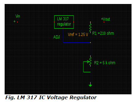 a.
a. 30.16 V & 1.25 V
b. 29.66 V & 0 V
c. 27.99 V & 0 V
d. 31.49 V & 1.25 V
|
Answer
Explanation
|
ANSWER: 31.49 V & 1.25 V
Explanation:
According to the equation of output voltage for IC voltage regulator,
Vout = Vref [1+ (R2/ R1)] + IADJ R2
Considering R2 at its minimum value = 0 ohm, the output voltage is evaluated by,
Vout (min) = 1.25 [1 + (0 / 210 )] + (98.5 x10-6) x 0
= 1.25 V
For maximum value of R2 = 5 k ohm, the output voltage is,
Vout (max) = 1.25 [1 + (5 x 10³ / 210)] + (98.5 x 10⁻⁶ ) x 5 x 103
= 1.25 [1+ (5000 / 210)] + (98.5 x 10 - 6) x 5000
= 31 + 0.4925
= 31. 49 V
|
|
10) Which circuit has the potential to overcome the drawback of unprotected external pass transistor from the excessive current from a shorted output in linear voltage regulators?
a. Current Regulator
b. Current Limiter
c. Voltage Regulator
d. Voltage Limiter
|
Answer
Explanation
|
ANSWER: Current Limiter
Explanation:
The current sensing resistor sets base-to-emitter voltage of transistor in current-limiting circuit, by evaluating the difference between the voltage across the external resistor and voltage across limiting resistor due to opposite polarities. If the value of current through the external pass transistor increases beyond maximum value due to shorted output, then the value of voltage across the limiting resistor reaches to 0.7V by turning ON the current limiting transistor.
Hence, it becomes feasible for the current limiting transistor to conduct the current away from the external pass transistor as well as regulator. This ultimately results in an occurrence of thermal overload to some extent by shutting down the regulator. Factually, overall internal protection of IC voltage regulator from thermal overload is a major stage taken into consideration from designing point of view.
|
|


